
(© Iwona joanna Rajszczak | Dreamstime.com)
OSAKA, Japan — The future of computer memory might not lie in electrical currents, but in the precise manipulation of magnetic fields. Scientists at Osaka University have demonstrated a novel approach to storing digital information that could dramatically reduce the power consumption of everything from smartphones to data centers, while maintaining the speed and reliability we’ve come to expect from modern devices.
As memory demands continue to grow in our increasingly digital world, this development marks a significant step toward more efficient and sustainable computing technologies. Like the transition from mechanical to electronic calculators, this breakthrough, detailed in Advanced Science, could herald a new era in how we store and process information.
The advancement centers on a technology called Magnetoresistive Random-Access Memory (MRAM), which has emerged as a promising candidate for next-generation computer memory due to its speed, durability, and compatibility with existing semiconductor manufacturing processes. Traditional computer memory faces a significant challenge: it requires constant power to maintain stored information, similar to how a light bulb needs continuous electricity to stay lit. MRAM, however, uses magnetic states to store information, making it non-volatile – meaning it maintains stored data even when powered off, much like how a refrigerator magnet keeps its magnetic properties without any power source.
“As MRAM devices rely on a non-volatile magnetization state rather than a volatile charge state in capacitors, they are a promising alternative to DRAM in terms of their low power consumption in the standby state,” says lead author Takamasa Usami in a statement.
Current MRAM technology faces its own challenges, particularly in how data is written to the memory. Traditional MRAM devices rely on electric currents to write data, but this approach becomes increasingly problematic as devices get smaller, requiring more power to operate effectively. The process also generates heat through what’s known as Joule heating, further increasing energy consumption – imagine trying to write with a pencil that gets hotter and heavier as the paper gets smaller.
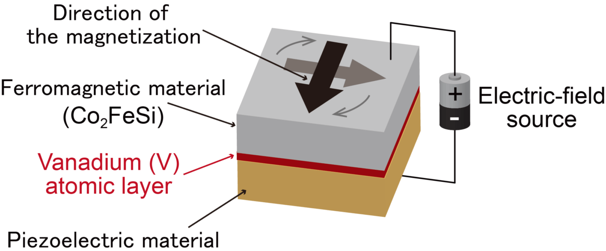
The research team tackled this challenge by creating a specialized layered structure combining a magnetic material called Co2FeSi with a piezoelectric crystal known as PMN-PT. When an electric field is applied to this combination, it creates mechanical strain that can flip the magnetization direction in the Co2FeSi layer – essentially writing a digital bit of information without using electric current. This approach is more like using a rubber stamp: regardless of size, it requires the same modest amount of pressure to make an impression.
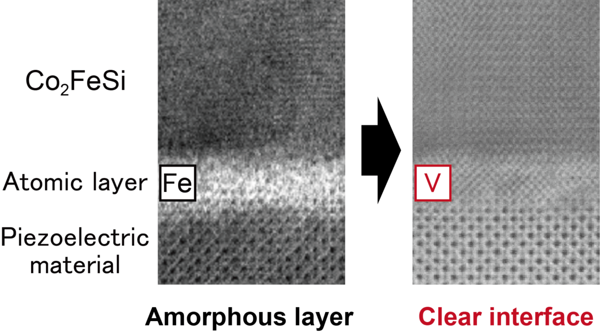
The researchers achieved a particularly strong version of this effect, known as the magnetoelectric effect, by carefully engineering the crystal structure of their materials. They discovered that by inserting an ultra-thin layer of vanadium between the magnetic and piezoelectric layers, they could enhance the interaction between them significantly and improve the overall stability of the device.
Think of the team’s innovation as being able to flip a microscopic compass needle using an electric field rather than another magnet. By carefully adjusting the thickness of both the vanadium and Co2FeSi layers – down to measurements just a few atoms thick – they achieved precise control over this magnetic switching behavior. This fine-tuning capability allowed them to achieve what’s known as a “giant” magnetoelectric effect, measuring over 10^-5 seconds per meter – surpassing the performance of similar devices without the vanadium layer.
With the demonstration of this new memory technology, researchers have shown that the future of computing doesn’t necessarily require choosing between performance and efficiency. By harnessing the interaction between electric fields and magnetic materials, they’ve opened up new possibilities for memory devices that could transform everything from mobile devices to large-scale computing infrastructure.
Paper Summary
Methodology Explained
The researchers created their device by building up layers of materials using a technique called molecular beam epitaxy. They started with a piezoelectric PMN-PT crystal, added an ultra-thin layer of vanadium (ranging from 0.3 to 2 nanometers thick), and topped it with a layer of Co2FeSi (varying from 10 to 30 nanometers thick). They then used various analytical techniques, including X-ray diffraction and electron microscopy, to study the crystal structure and magnetic properties of their samples.
Results Breakdown
The team found that their device exhibited the strongest magnetoelectric effect when using a 0.3-nanometer-thick vanadium layer and a 30-nanometer-thick Co2FeSi layer. Under these conditions, they achieved a magnetoelectric coefficient exceeding 10^-5 seconds per meter, while maintaining distinct magnetic states at zero electric field. The system demonstrated reliable switching behavior and stability at room temperature.
Limitations
While promising, the research was conducted using relatively large crystal substrates. Scaling the technology down to the size needed for commercial memory devices will require additional development. The study also focused primarily on fundamental physical properties rather than practical device implementation.
Discussion and Takeaways
The research demonstrates a viable pathway toward more energy-efficient memory devices. The ability to control magnetization using electric fields rather than currents could significantly reduce power consumption in future computer systems. The team’s approach of using vanadium as an interface layer provides a new tool for engineering similar magnetoelectric systems.
Funding and Disclosures
The research was supported by various Japanese funding agencies, including the Japan Science and Technology Agency CREST program and the Japan Society for the Promotion of Science KAKENHI grants. The authors declared no conflicts of interest.
Publication Information
The study, titled “Artificial Control of Giant Converse Magnetoelectric Effect in Spintronic Multiferroic Heterostructure,” was published in Advanced Science in 2024. The research was conducted by scientists from Osaka University’s Center for Spintronics Research Network and related departments.


